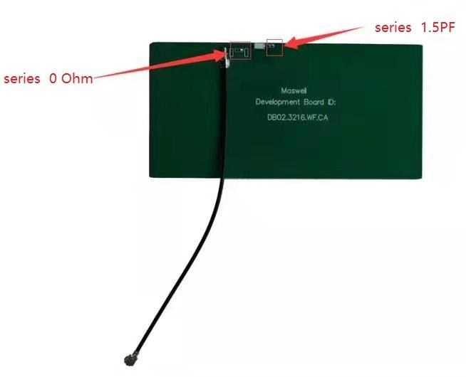
Maswell launched a development board (ID:DB02.3216.WF.CA) for its 3216 WiFi Chip antenna. The test and matching circuit of this chip antenna uses 3216 PCB foot print. The detailed PCB design file is available for download from the Maswell official website below: http://www.maswelltech.com/index.php?m=content&c=index&a=show&catid=45&id=276
Figure 1. Product Diagram
Product Parameters of DB01.3216.WF.CA:
| Item |
Specifications |
| Antenna |
Gain |
2dBi |
| Mechanical |
Dimension |
100*40*1mm |
| Cable |
10cm |
| Connector |
ipex |
| Material |
FR4 |
Figure 2. PCB design macro image
In the test circuit and matching circuit, the chip uses 3216 PCB foot print with a operating frequency of 2400~2500MHz. Overall the antenna on the breadboard has a gain of 2dBi, VSWR of 2.0, a linear polarization and omnidirectional patterns. In the series circuit of the PCB design, it uses series 0 Ohms (direct line connection) and series 1.5PF lumped capacitor. The actual design parameters in practical applications can be tuned accordingly to fit the application requirements.
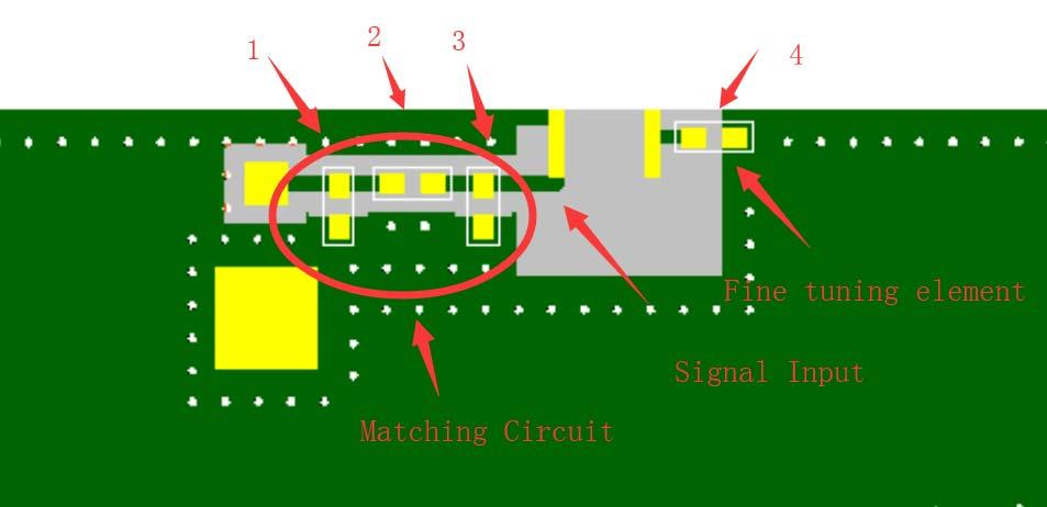
Figure 3. PCB design details

Figure 4. Evaluation Board and Matching Circuits
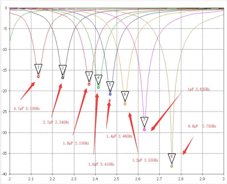
Figure 5. The echo loss under different capacitances