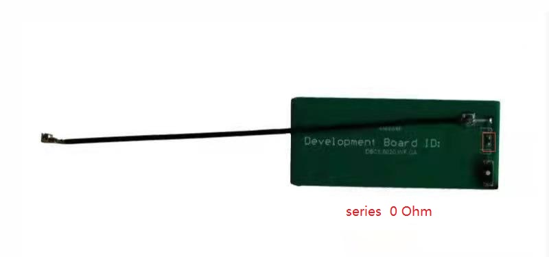
Maswell launched a development board DB01.5020.WF.CA for our new SMD chip antenna 5020 series. In this board design, the antenna uses 5020 PCB foot print for the testing and matching circuit. For detailed PCB design file, please visit Maswell official website via the URL below: http://www.maswelltech.com/index.php?m=content&c=index&a=show&catid=45&id=277
Figure 1. Product Diagram
Product Parameters of DB01.5020.WF.CA:
Item
Specifications
Antenna
Gain
2dBi
Mechanical
Dimension
100*40*1mm
Cable
10cm
Connector
ipex
Material
FR4
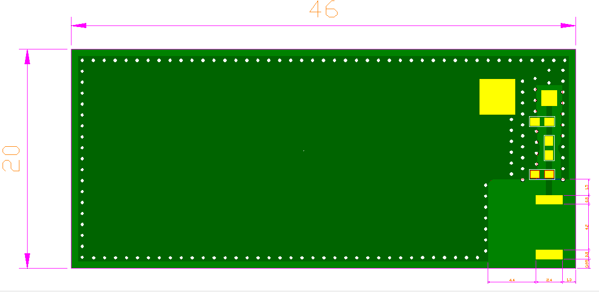
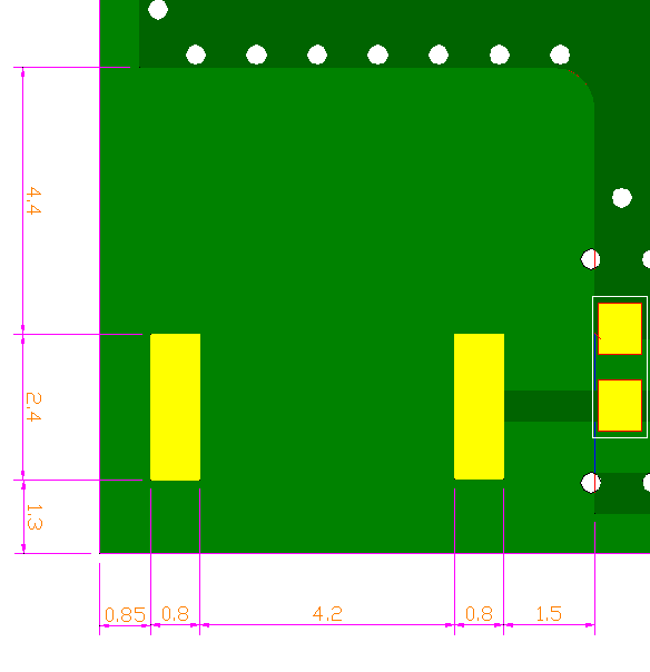
Figure 2. PCB design macro image
The design and matching circuit uses 5020 PCB foot print with an operating frequency of 2400~2500MHz. The test board antenna has a gain of 2dBi, VSWR of 2.0, linear polarization and omnidirectional radiation patterns. A direct line connection is used to demonstrate 0 Ohms resistor in the design scheme.